FSK digital signalling is one of the methods in which a digital signals can be converted into higher frequency signals and transmitted over a channel which requires higher frequencies. In this post, it is shown how FSK modulation can be achieved using the 74HC4046 PLL/ VCO IC. The simulation is done in Proteus ISIS.
Here only the VCO part of the IC is used for the frequency modulation. Digital stream of data enters the VCO and we get FSK signal at the VCO output.
The frequencies of the VCO is set using three external components- one capacitor C1 and two resistors R1 and R2.
However R2 is optional which is only used to set the frequency offset if it is used.
So here first frequency modulation without frequency offset, that is no R2 and then frequency modulation with the frequency offset using R2 is shown.
First without R2 resistor.
The circuit diagram below shows implementation of FSK modulation using the 74HC4046 PLL/ VCO IC in Proteus.
The data enters the port VCOIN which is pin 9. The data is digital one with 1V(or 0V) for logic 0 and 4.5V for logic 1. The data rate of this stream is 500bps and therefore the frequency of the signal is 250Hz.
The value of capacitor C1 and resistor R1 determines the frequencies of the FSK modulation. These frequencies were 800KHz and 12KHz. Accordingly the center frequency is 10KHz. We can then use the following graph to get the values of C1 and R1 which were taken to be 2.5nF and 220Kohm at the supply voltage of 4.5V.
 In the digital waveform graph we get the following graph for the output FSK signal,

We can see the two square waves corresponding to the two different frequencies.
Similarly viewing the output FSK signal in the analog graph we get the following signal waveform showing the two different frequencies(zoomed in view).

In the first illustration of the FSK modulation the frequency offset was not used and therefore the resistor R2 was not connected, that is, it was left open.
Now the following shows how R2 can be connected to set an offset frequency and get FSK modulation output.

The value of C1, R1 and R2 were determined as follows.
First we determine the frequency offset using the equation,
frequency offset = center frequency - 1.6*frequency lock
foff = fo - 1.6*fl
since fo = 10KHz and 2*fl=4KHz and therefore fl = 2KHz
we find that, foff = 6.8KHz
Now we use this value of foff to determine C1 and R2 using the following graph,
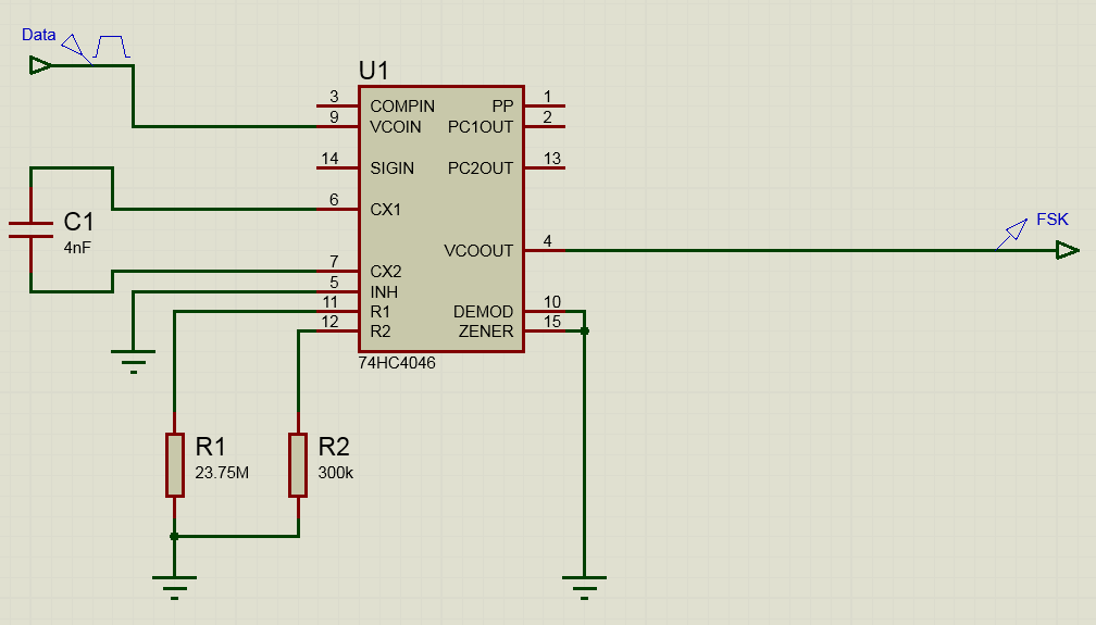
 which gives us C1=4nF, R2 = 300KOhm.
Now what remains is to find out the value of R1
We first calculate the frequency lock range which is the difference between the maximum frequency and the minimum frequency which are 12KHz and 8KHz respectively. This gives us the frequency lock range which is (12-8)=4KHz.
Using this frequency lock range we can determine the product R1*C1 using the following graph.

which is approximately R1*C1 = 9.5*10^-2
Now we know that C1 is 4nF so we can determine R1 from the relation above which gives us,
R1 = 23.75MOhm
These values of C1, R1 and R2 were used in the above schematic.
Now the graph obtained from simulation is shown.
Analog Graph result-

Digital Graph result-

The above two graph basically shows two types of waveform corresponding to two frequencies of FSK signal.
Here only the VCO part of the IC is used for the frequency modulation. Digital stream of data enters the VCO and we get FSK signal at the VCO output.
The frequencies of the VCO is set using three external components- one capacitor C1 and two resistors R1 and R2.
However R2 is optional which is only used to set the frequency offset if it is used.
So here first frequency modulation without frequency offset, that is no R2 and then frequency modulation with the frequency offset using R2 is shown.
First without R2 resistor.
The circuit diagram below shows implementation of FSK modulation using the 74HC4046 PLL/ VCO IC in Proteus.
 |
| FSK modulation using 74HC4046 PLL/ VCO IC |
The data enters the port VCOIN which is pin 9. The data is digital one with 1V(or 0V) for logic 0 and 4.5V for logic 1. The data rate of this stream is 500bps and therefore the frequency of the signal is 250Hz.
The value of capacitor C1 and resistor R1 determines the frequencies of the FSK modulation. These frequencies were 800KHz and 12KHz. Accordingly the center frequency is 10KHz. We can then use the following graph to get the values of C1 and R1 which were taken to be 2.5nF and 220Kohm at the supply voltage of 4.5V.


We can see the two square waves corresponding to the two different frequencies.
Similarly viewing the output FSK signal in the analog graph we get the following signal waveform showing the two different frequencies(zoomed in view).

In the first illustration of the FSK modulation the frequency offset was not used and therefore the resistor R2 was not connected, that is, it was left open.
Now the following shows how R2 can be connected to set an offset frequency and get FSK modulation output.

The value of C1, R1 and R2 were determined as follows.
First we determine the frequency offset using the equation,
frequency offset = center frequency - 1.6*frequency lock
foff = fo - 1.6*fl
since fo = 10KHz and 2*fl=4KHz and therefore fl = 2KHz
we find that, foff = 6.8KHz
Now we use this value of foff to determine C1 and R2 using the following graph,

Now what remains is to find out the value of R1
We first calculate the frequency lock range which is the difference between the maximum frequency and the minimum frequency which are 12KHz and 8KHz respectively. This gives us the frequency lock range which is (12-8)=4KHz.
Using this frequency lock range we can determine the product R1*C1 using the following graph.

which is approximately R1*C1 = 9.5*10^-2
Now we know that C1 is 4nF so we can determine R1 from the relation above which gives us,
R1 = 23.75MOhm
These values of C1, R1 and R2 were used in the above schematic.
Now the graph obtained from simulation is shown.
Analog Graph result-

Digital Graph result-

The above two graph basically shows two types of waveform corresponding to two frequencies of FSK signal.
0 comments:
Post a Comment